Sign up for our newsletter!
Your data will be handled in compliance with our privacy policy.
Your data will be handled in compliance with our privacy policy.

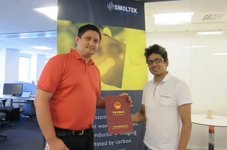
Smoltek has yet another granted patent to add to its extensive IP portfolio. This patent, the 49th of the company’s granted patents, is regulating patent rights on nanostructure processing in China.
The new Chinese patent strengthens the position of our helplayer patent family towards forming of nanostructure devices. The method covers different types of nanostructures including carbon nanotubes, nanofibers, nanowires etc.
“Another confirmation of our unique nanostructure growth platform technology that enables manufacturing of nanomaterial devices on CMOS platform. We are humbled to see that our IP footprint is constantly strengthening in China, one of the main hubs for semiconductor manufacturing”, says Dr. M. Shafiq Kabir, Smoltek´s CIO.
Smoltek’s patent portfolio now globally comprises 49 granted patents.
Your data will be handled in compliance with our privacy policy.

Smoltek Hydrogen has appointed Shafiq Kabir as Head of Volume Processes. Shafiq is the founder of Smoltek and he methodically created the company's technology platform and patent portfolio until January 2021, when he took a break from the nanotechnology industry for pursuing an Executive MBA-program.

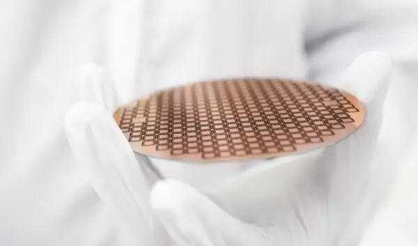
Smoltek holds unique world patents for technologies that make material engineering on an atomic level possible. Smoltek has solutions that allow continued miniaturization and increased performance of semiconductors, contribute to carbon-free steel production and renewable energy storage, and enable mind control of robotic prostheses. This is a story of how Smoltek came to be.

Smoltek has been granted three new patents since the start of the year. The patents are related to three different families: Interconnects, Assembly platform and Compact energy storage interposer. This makes our patent portfolio to now comprise 68 granted patents in total.

Smoltek has yet another patent granted. This time in India. The patent is related to the growth process of nanostructures and it makes the Catalyst diffusion patent family complete.
The constantly expanding Smoltek IP-portfolio is divided into several different patent families. One of them is named Helplayer, a method to protect the underlaying materials when growing nanostructures on a given surface. To this family we can add another patent number recently granted.
Smoltek is awarded a new patent. This Korean patent is the second of a patent family in the direction of CNF-MIM based compact energy storage interposers. This means that our patent portfolio now comprises 56 granted patents.