Search Results for Hot C-TS452-2022 Free Braindumps | Professional C-TS452-2022 Pass Exam: SAP Certified Application Associate - SAP S/4HANA Sourcing and Procurement 🦐 Simply search for ➥ C-TS452-2022 🡄 for free download on ➡ www.pdfvce.com ️⬅️ 🔱Answers C-TS452-2022 Real Questions
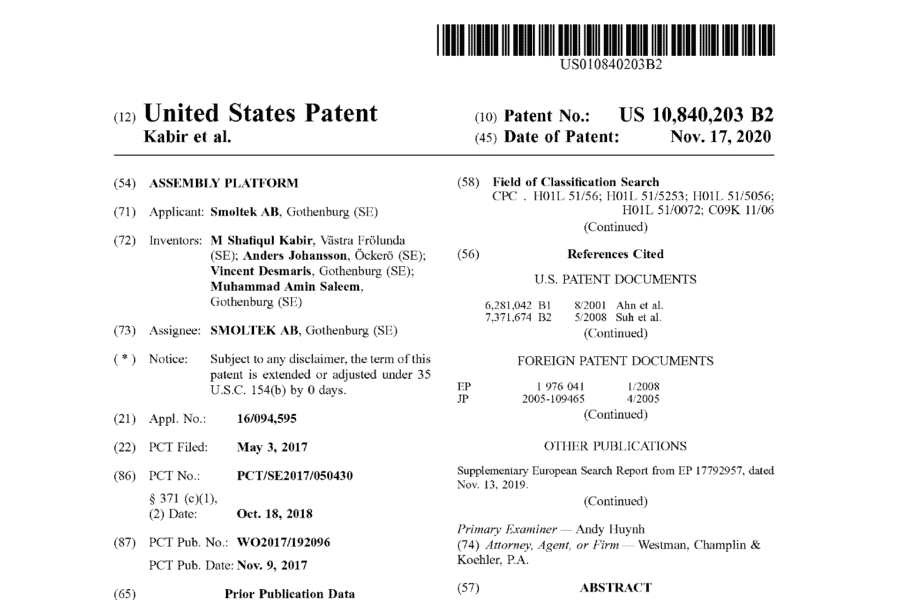
The invention: An assembly platform for arrangement as an interposer device between an integrated circuit and a substrate to interconnect the integrated circuit and the substrate through the assembly platform, the assembly platform comprising: an assembly substrate; a plurality of conducting vias extending through the assembly substrate; at least one nanostructure connection bump on a first side of...
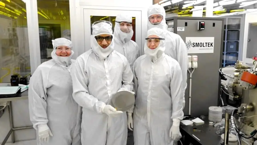
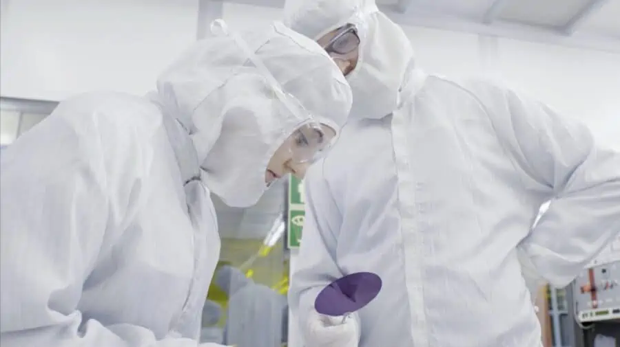
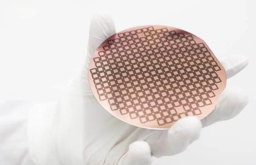
...available tools and materials, and ensure the fastest, easiest, and smoothest process possible. We have come a long way in doing so. We have now implemented a process with our partners that enables us to produce high-volume engineering samples. 3. Standard tools and 8‑inch wafers An example of adaptation we have made going from the lab to...
Gender equality plan Smoltek as a group is committed to a sustainable future by developing carbon nanotechnology solutions that improve the properties of advanced and expensive materials that enables reduced energy consumption, lower operating costs that supports the transition to a carbon neutral society. Including Smoltek’s sustainable development goals, gender equality and equal treatment are also essential for...
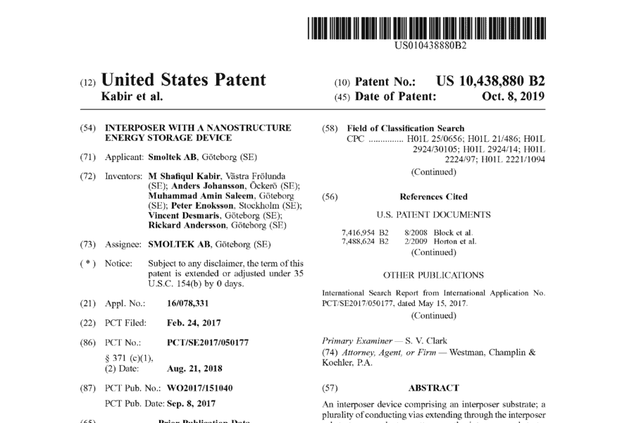
The invention: An interposer device comprising an interposer substrate; a plurality of conducting vias extending through the interposer substrate; a conductor pattern on the interposer substrate, and a nanostructure energy storage device. The nanostructure energy storage device comprises at least a first plurality of conductive nanostructures formed on the interposer substrate; a conduction controlling material embedding each nanostructure in the...
...carbon nanofiber technology. Smoltek conducts operations in the development, industrialization and licensing of technology solutions, based on the company’s patent-protected carbon nanofiber technology, for the semiconductor industry within the Group company Smoltek Semi. Its main focus is the industrialization and commercialization of the company’s ultra-thin CNF-MIM capacitors. The company has one active agreement for industrial...
The invention: Integrated circuit comprising nanostructures. The present invention provides for nanostructures grown on a conducting substrate, and a method of making the same. The nanostructures grown according to the claimed method are suitable for interconnects and heat dissipators in electronic devices. Download the patent granted by EPO. Granted patents relating to the innovation Patent OfficePatentChina CN101189372 China...
...carbon nanofiber technology. The company’s technology solutions for the Semiconductors business area are developed by the Group company Smoltek Semi. The focus is on industrializing and commercializing the company’s ultra-thin CNF-MIM capacitors. Fredrik Liljeberg 0 0 Smoltek has placed an order on an industrial carbon growth machine – Smoltek After completed tests and evaluations, Smoltek Semi...
Electronica 2022 and SEMICON Europe are held in Munich, Germany, 15–18 November. This is the first time they are co-located, and together they form the largest event and trade fair for electronics manufacturers in Europe. Smoltek will participate together with Yageo, and present the two company’s joint collaboration for industrializing and commercializing ultra-thin capacitors that...
Smoltek has entered into negotiations with Imec, the world-leading research institute, on demo production of CNF-MIM capacitors in industrially compatible CMOS format, so-called 300mm format. - Imec is a unique player with a complete and industrially compatible 300mm line, under one roof. They also have experience in the field of carbon nanotechnology, which we see as an...
...machine and industrial silicon foundry processes. “We are excited to partner with a major passive component manufacturer to commercialize a product that is based on our core Carbon Nanofiber technology. We now have a perfect partner in place to complete a competitive product and industrial mass production process for our ultra-thin CNF-MIM capacitors” says Smoltek’s CEO Håkan Persson The...
The invention: An apparatus comprising two conductive surfaces or layers and a nanostructure assembly bonded to the two conductive surfaces or layers to create electrical or thermal connections between the two conductive surfaces or layers, and a method of making same. Download the patent granted by EPO. Granted patents relating to the innovation Patent OfficePatentChina CN101827782 China CN104600057 Europe...