Sign up for our newsletter!
Your data will be handled in compliance with our privacy policy.
Your data will be handled in compliance with our privacy policy.


Smoltek Semi has developed a new material for use in CNF-MIM capacitors. The new material increases capacitance by more than three times and reduces leakage current by 50 percent. In this article, we examine what this means and why it is good for shareholders and investors.
In a press release, we announced that Smoltek Semi has developed a new dielectric stack that increases capacitance density by 230 percent and reduces leakage current by 50 percent. But what the heck is a dielectric stack? And how does it benefit you as a shareholder and investor?
Carbon nanofibers are the core of what we do. We use them to tackle complex material challenges across various industries, such as creating ultra-thin capacitors with sufficient capacitance.
Capacitors are essential for stabilizing the power fluctuations caused when transistors inside an application processor switch between ones and zeros billions of times per second. They quickly absorb excess energy and release stored energy when needed. The catch is that these capacitors must be placed very close to the transistors to be effective—ideally, right under the chip itself.
This requires capacitors small enough to fit between the solder balls on the underside of the chip. These capacitors need to be thinner than the diameter of the solder balls yet still provide enough capacitance to handle the task.
Smoltek Semi addresses this challenge with its CNF-MIM capacitors.
Fundamentally, a capacitor consists of two metal plates with an insulating material between them. Its ability to store energy, capacitance, is primarily determined by three factors:
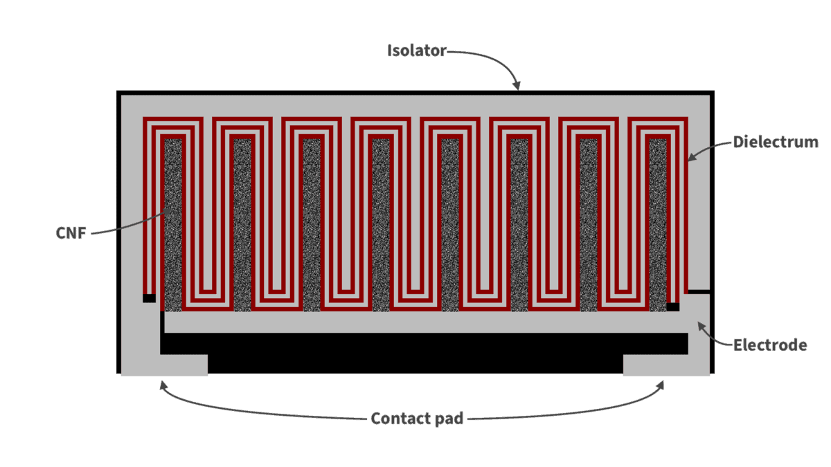
CNF-MIM capacitors are just metal-insulation-metal (MIM) capacitors where we create a large area in a small volume using carbon nanofibers (CNF).
Growing carbon nanofibers on a surface increases the surface area tens of thousands of times. To understand why this is so, consider a carbon nanofiber as a vertically standing cylinder of height h and radius r. The cylinder’s mantle surface is 2πrh, and its base surface is πr2. So you could say that the carbon nanofiber takes up a surface of πr2 but creates a new surface of 2πrh. Since h is much larger than r, the new surface is also much larger, more precisely 2πrh / πr2 = 2h/r. A carbon nanofiber with r = 20 nm and h = 20 µm thus increases the area by a whopping factor of 1,000.
It is this capacity, as an area multiplier, that carbon nanofiber is used in Smoltelk’s CNF-MIM capacitor. They multiply the surface area, which we then cover layer by layer with metal, insulation, and more metal.
Simply put, we start with a substrate on which we grow a forest of carbon nanofibers. Each carbon nanofiber is then coated in metal. Next, we add a layer of insulation over the metal-coated nanofibers. Finally, we place another metal layer on top of the insulation. This creates a large metal-insulation-metal surface area relative to its small volume.
Because a capacitor’s ability to store energy is proportional to its surface area, the capacitance per unit volume of CNF-MIM capacitors is extremely high. This allowed Smoltek to showcase a lab prototype of the world’s thinnest capacitor already in 2021.
Hafnium oxide was used as insulation in the first batches of CNF-MIM capacitors. Hafnium oxide is a material with high dielectric constant κ.
What the press release says is that Smoltek Semi’s researchers have developed a brand new insulation that alone increases capacitance density by 230 percent compared to hafnium oxide.
On the same surface area as before, we can now get more than three times the capacitance. This means that Smoltek puts further distance between itself and its competitors.
Moreover, as icing on the cake, Smoltek’s engineers have reduced the inevitable leakage current by 50 percent.
The new insulation consists of layer upon layer of two materials. One material has a very high dielectric constant κ, which means it can store a lot of energy. The other material is a very good electrical insulator, which means it acts as a barrier to leakage current.
We call the new material a dielectric stack, because it is a stack of layers of the two materials, and it has a high dielectric constant κ.
To better understand the properties of the new dielectric stack, we began by using it in the simplest type of capacitors: parallel plate capacitors. As the name suggests, these consist of two parallel metal plates with the dielectric stack between them. This design lets us study the dielectric stack’s characteristics without interference from other factors.
We have manufactured these capacitors and sent them to Yageo for reliability testing and further characterization. Meanwhile, we’ve already moved on to the next phase: integrating the new dielectric stack into CNF-MIM capacitors.
As Yageo carries out its testing and the first CNF-MIM capacitors are produced using the new dielectric stack, Smoltek’s CTO, Farzan Ghavanini, reviews the initial results with satisfaction and enthusiasm. With a 230 percent increase in capacitance, a 50 percent reduction in leakage current, and a flawless 100 percent fabrication yield, he is genuinely thrilled by this breakthrough.
So, what does this mean for you as a shareholder and investor?
This means that Smoltek is not just keeping up in a competitive industry but also actively pulling ahead. With a 230 percent increase in capacitance and a 50 percent reduction in leakage current, Smoltek has set a new benchmark in performance. This breakthrough strengthens our market position and makes our technology even more attractive to major players in the semiconductor industry. It’s not just a technical achievement—it’s a commercial advantage that could lead to new partnerships and a faster path to market adoption.
Your data will be handled in compliance with our privacy policy.

In an age where environmental sustainability is of utter importance, it is crucial to find innovative solutions to reduce energy consumption and minimize our carbon footprint. One such solution is found in capacitors. These unassuming electronic components not only play an important role in various systems, but also offer significant environmental benefits. Albeit very small – if counted one by one.

In the race to make green hydrogen economically viable, researchers worldwide are pursuing the seemingly impossible: reducing iridium use in PEM electrolyzers by 95%. As Smoltek gets closer to this holy grail of 0.1 mg/cm², we examine how other technologies measure up.

When experts talk about the energy systems of the future, they often come back to one specific number: 0.1 milligrams per square centimeter (0.1 mg/cm²). This seemingly insignificant number could be critical to moving green hydrogen from a promising concept to an economic reality.

Modern electronics demand increasingly compact and powerful capacitors, and the race for miniaturization has reached a critical juncture. While both Deep Trench Capacitors (DTC) and Carbon Nanofiber Metal-Insulator-Metal (CNF-MIM) capacitors are being developed for advanced applications requiring smaller size and higher capacitance density than conventional surface-mounted capacitors, DTC pushes the boundaries of what’s achievable with subtractive manufacturing, but is hitting fundamental physical limits. In contrast, Smoltek’s innovative CNF-MIM technology offers a revolutionary path forward, unrestricted by these constraints.

An interview with Smoltek Hydrogen CEO Ellinor Ehrnberg about her recent visit to Germany and the rapid acceleration of the hydrogen economy.

Leading PEM technology expert Dr. Felix Büchi has completed an independent assessment of Smoltek Hydrogen’s Porous Transport Electrode (PTE) technology, confirming its unique ability to dramatically reduce iridium usage while maintaining high performance in hydrogen production. In an exclusive interview with Smoltek Hydrogen’s President, Ellinor Ehrnberg, Büchi shares insights about the technology’s distinctive advantages and market potential.