Sign up for our newsletter!
Your data will be handled in compliance with our privacy policy.
Your data will be handled in compliance with our privacy policy.

The Helplayer family is covering a method to protect the underlaying substrate or materials from being damaged during the nanostructure growth process.
The invention: A method for making one or more nanostructures is disclosed, the method comprising: depositing a conducting layer on an upper surface of a substrate; depositing a patterned layer of catalyst on the conducting layer; growing the one or more nanostructures on the layer of catalyst; and selectively removing the conducting layer between and around the one or more nanostructures. A device is also disclosed, comprising a substrate, wherein the substrate comprises one or more exposed metal islands separated by one or more insulating areas; a conducting helplayer disposed on the substrate covering at least some of the one or more exposed metal islands or insulating areas; a catalyst layer disposed on the conducting helplayer; and one or more nanostructures disposed on the catalyst layer.
| Patent Office | Patent |
|---|---|
| China | CN102007571 |
| China | CN105441903 |
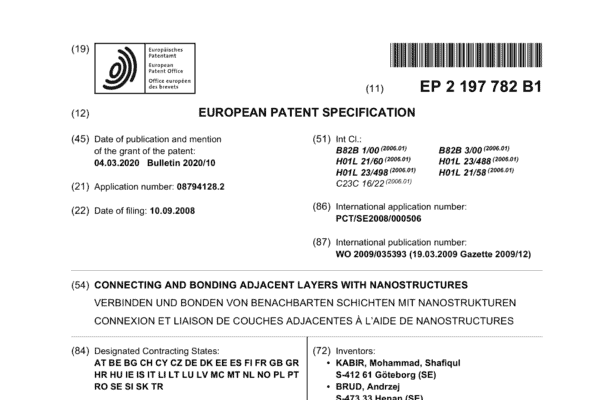
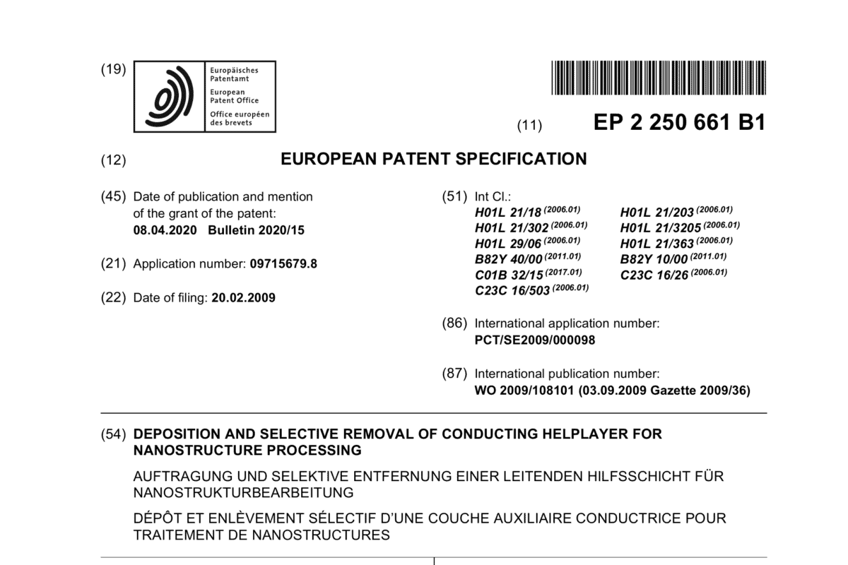
| Europe | EP2250661 |
| India | IN327303 |
| Japan | JP5474835 |
| Japan | JP5943947 |
| Japan | JP6126725 |
| South Korea | KR101638463 |
| Taiwan | TWI465389 |
| USA | US8508049 |
| USA | US8866307 |
| USA | US9114993 |
Your data will be handled in compliance with our privacy policy.
The constantly expanding Smoltek IP-portfolio is divided into several different patent families. One of them is named Helplayer, a method to protect the underlaying materials when growing nanostructures on a given surface. To this family we can add another patent number recently granted.
Smoltek keep growing its proprietary technology platform. In the beginning of May 2020 patent No. 58 was granted. The patent is connected to our helplayer family.
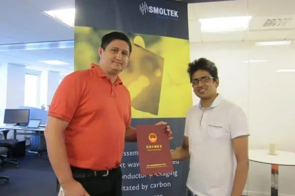
Smoltek has yet another granted patent to add to its extensive IP portfolio. This patent, the 49th of the company’s granted patents, is regulating patent rights on nanostructure processing in China.
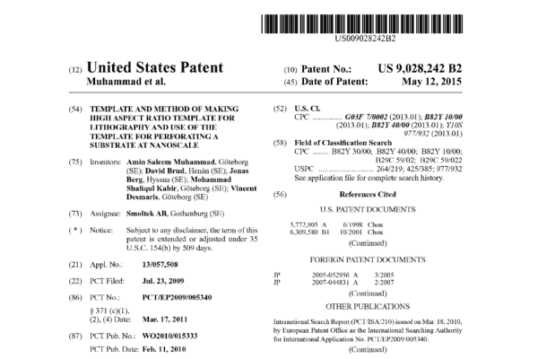
The Nano Imprint Lithography family is covering a method of making high aspect ratio template, stamp, and imprinting at nanoscale using nanostructures.
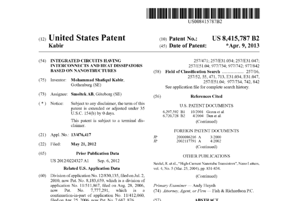
The Interconnects B family is covering how nanostructures can be used as interconnects and/or for dissipating heat from electronic devices.