Sign up for our newsletter!
Your data will be handled in compliance with our privacy policy.
Your data will be handled in compliance with our privacy policy.

The constantly expanding Smoltek IP-portfolio is divided into several different patent families. One of them is named Helplayer, a method to protect the underlaying materials when growing nanostructures on a given surface. To this family we can add another patent number recently granted.
This, our 61st patent, is granted in India which is a fast-growing market within the semiconductor industry. The patent belongs to the Helplayer family – one of our hardcore technology and concept families. The Helplayer technology essentially is a method to protect the underlaying substrate or materials from being damaged during the nanostructure growth process.
India is a fast-growing semiconductor market in the field of consumer electronics. Furthermore, India is emerging as a new important semiconductor fab source in Asia. Hence it becomes a strategic choice to have a core IP footprint also in India.”, says Dr Shafiq Kabir, Founder and Chief Innovation Officer at Smoltek.
Smoltek’s patent portfolio has today developed into several patent families, starting from fundamental technology that enables controlled growth of nanostructures. Since then, the portfolio has further expanded into the domain of devices/components based on, or enabled by, nanostructures.
During the initial phase of Smoltek’s development of intellectual property, the first set of patent families was designed to protect essential industry-compatible processes. One of these early families is a method patent family named Helplayer.
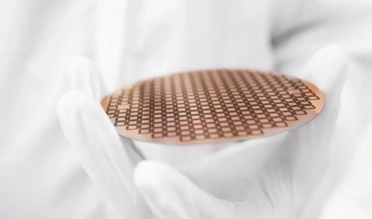
The Helplayer patent family offers a method to protect the underlying substrate and materials when growing nanostructured material on the surface. Subsequently, afterwards the helplayer can be removed from the unwanted areas in a controlled way without damaging underlaying materials, or circuits (i.e. transistors). This method, for example, provides the possibility to manufacture smaller and thinner high-performance capacitors not only as discrete capacitor components but also as integrated capacitors at wafer fab production of for example microprocessors, smart interposers or chiplets.
Smoltek’s patent portfolio now globally comprises 61 granted patents. Read more about our IP and patents.
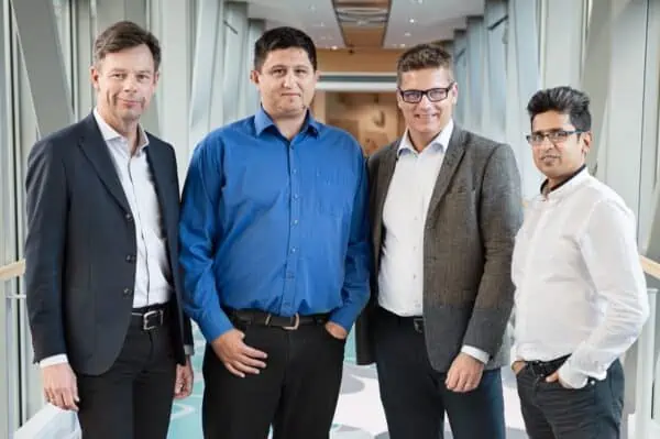
Image: Shafiq Kabir, CIO at Smoltek
Your data will be handled in compliance with our privacy policy.
Smoltek’s 75th patent has been granted in Taiwan and is covering the concept and manufacturing of extremely thin energy storage devices embedded in an interposer. The energy storage device concepts ...
Smoltek holds unique world patents for technologies that make material engineering on an atomic level possible. Smoltek has solutions that allow continued miniaturization and increased performance of semiconductors, contribute to carbon-free steel production and renewable energy storage, and enable mind control of robotic prostheses. This is a story of how Smoltek came to be.

Smoltek has been granted three new patents since the start of the year. The patents are related to three different families: Interconnects, Assembly platform and Compact energy storage interposer. This makes our patent portfolio to now comprise 68 granted patents in total.

Smoltek has yet another patent granted. This time in India. The patent is related to the growth process of nanostructures and it makes the Catalyst diffusion patent family complete.

Smoltek’s proprietary platform keeps growing as we have been awarded another approved patent. This new US patent covers energy storage devices and the usage of the same. Our patent portfolio now comprises 60 granted patents.
Smoltek keep growing its proprietary technology platform. In the beginning of May 2020 patent No. 58 was granted. The patent is connected to our helplayer family.