Sign up for our newsletter!
Your data will be handled in compliance with our privacy policy.
Your data will be handled in compliance with our privacy policy.

With our carbon nanofibers (CNFs) fabrication technology, we develop advanced packing solutions and ultra-miniaturized capacitors for use in the semiconductor industry.
Based on our CNF-technology, we have developed an assembly platform that pushes the limits for heterogeneous integration in 2.5D and 3D. The platform offers ultra-fine pitch microbumps, ultra thin thermal film for heat dissipation, ultra miniaturized capacitors integrated directly onto dies or embedded into interposers, and an interposer with built-in DC storage smoothing out variations in power supply.
We have also developed the world’s smallest capacitor. The total height is only 30 µm—which is less than half what is possible with other technologies. Its capacitance is a whopping 650 nF/mm2. Its internal resistance (ESR) is less than 40 mΩ, and its internal inductance (ESL) is below 15 pH.
We offer a technical partnership to manufacturers who want to develop their offer in heterogeneous integration or passive components with our technology to shorten development time and minimize risks. Are you interested? Contact us now to learn more.
A material is an electrical conductor if an electric field can move an electron from one atom to the next. Only the electron in the outermost shell around an atomic nucleus can do that, and only if there is an even further out shell that it can jump to with energy from the electric field.
If the distance between the outermost shell of electrons and the next shell is too great for electrons to jump out there, the substance is an electrical insulator.
For some materials, such as silicon, the gap is so small that some electrons can jump across the gap. When the electron crosses the gap, it leaves behind a hole. Under the influence of an electrical field, both the electron and the hole can move across the material. It conducts electricity, but poorly. That’s why such a substance is called semiconductor.
The conductivity can be dramatically improved by adding impurities in the form of other substances that add extra electrons or holes. This is called n‑doping and p‑doping, respectively.
A p‑n-junction is where p‑doped semiconductor meets n‑doped semiconductor. At p‑n-junctions, the magic happens that makes modern electronics possible.
Because there is an excess of electrons in the n‑doped semiconductor and a deficit of electrons (holes) in the p‑doped semiconductor, electrons diffuse from the n‑doped to the p‑doped semiconductor to reach equilibrium. This creates a region that is depleted of electrons and holes that can carry current. Consequently, the region is said to be a depletion region.
By applying a voltage across the p‑n junction one can cause the depletion region to increase (which blocks current from passing) or decrease (which allows current to pass). This is what is exploited in transistors.
A transistor acts like an electrically controlled tap. By gently turning the tap, more or less flow can be created. This feature is used in analog electronics to amplify signals. By quickly turning the tap on or off, “ones and zeros” are created in terms of current passing or not. This is the foundation of all digital electronics, not least computers.
The first transistor was created in December 1947 at the Bell Telephone Laboratories. A couple of years later, what we today think of as a transistor was invented. It consists of n‑doped or p‑doped semiconductors through which current is passed. The middle part of the semiconductor is replaced by a piece of semiconductor of the opposite type. It creates two p‑n junctions. By supplying current through the middle section, the width of the two depletion regions can be changed. Thus, a current through the middle section controls how much of the current through the transistor is allowed to pass. Since both negative and positive charges are moving (electrons and electron holes, respectively), it is called bipolar junction transistor (BJT).
A transistor controlled by an electric field instead of current is called a field-effect transistor (FET). While the BJT always consumes power, the FET consumes no power when its tap is unchanged (e.g., on or off). That’s perfect for creating energy-efficient digital electronics.
The first field-effect transistor was developed in 1953. But it had problems with leakaging current where p–n junctions intercept the surface.
In the late 1950s, Mohamed M. Atalla of Bell Telephone Laboratories discovered that a thin layer of insulating silicon dioxide on top of a semiconductor prevents leakage current. But how to make electric contact with a FET if an insulating layer covers its surface?
Mohamed M. Atalla and his colleague Dawon Kahng elegantly solved this. They added metal gates on top of the oxide layer where they wanted the connection. The stack of metal, oxide, and semiconductor form a parallel-plate capacitor. The metal gate is one electrode, the semiconductor underneath is the other electrode, and the thin silicon dioxide layer acts as the dielectric. The much improved FET was named metal-oxide-semiconductor field-effect transistor, or MOSFET for short.
One of the MOSFETs’ many benefits is that compared to BJTs they are relatively easy to produce. Therefore, it is better to use MOSFETs in integrated circuits. Dawon Kahng pointed this out in 1961.
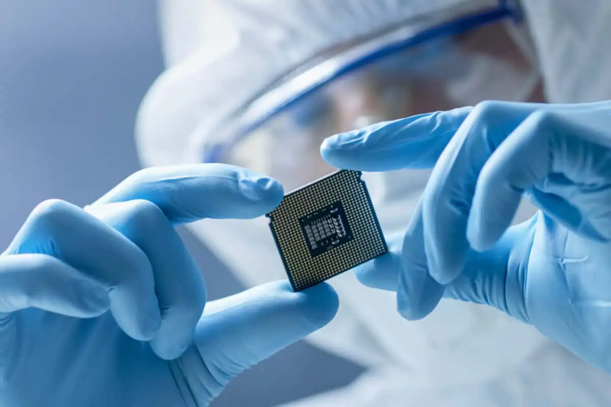
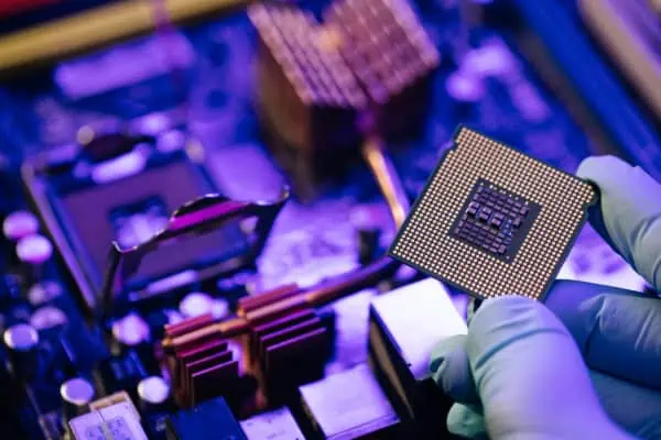
An integrated circuit (IC) is a set of electronic circuits on one small flat piece of semiconductor called chip. The idea of combining several components in one device goes back to 1949. But it wasn’t until a decade later that the first IC in a modern sense was fabricated. It used bipolar junction transistors (BJT). The first chip with MOSFET was fabricated in 1961.
MOSFETs are superior to BJTs in integrated circuits because they are easier to produce and can be made much smaller. It took only two years after the first MOSFET chip was produced before chips with MOSFET reached higher transistor density and lower manufacturing costs than those with BJTs.
In the late 1960s, the complementary metal-oxide-semiconductor (CMOS) was developed. The name refers to both a particular style of digital circuitry design, creating digital gates by combining two MOSFETs of opposite doping, and a process used to implement that circuitry on integrated circuits (chips). Two important characteristics of CMOS devices are high noise immunity and low static power consumption.
The production of chips is a complex process that can take up to three months. Today, they are usually manufactured according to the following steps:
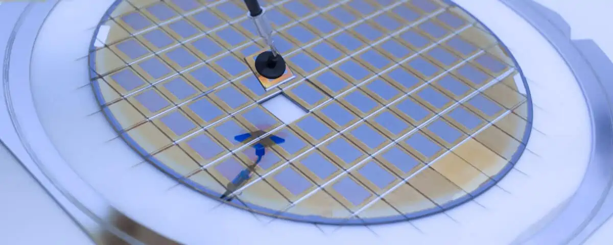
Although chip manufacturing has been refined since the first MOSFET chips were produced, not all dies will work. Therefore, each die must be tested (which is typically done before the wafer is diced). The percentage that passes is called the die yield.
The cost per transistor decreases with the number of transistors that fit on a chip to a point where the cost increases again due to decreasing yield. Thus there is an inflection point where the cost per transistor is the lowest possible.
In an article published in 1965 in Electronics (Volume 38, Number 8), Gordon E. Moore—co-founder of Fairchild Semiconductor and later Intel—referred to this optimal point as “minimum component costs.” Moreover, he noted that in those few years that chips had been produced, the number of transistors giving minimum component costs had doubled each year. He predicted that this growth rate would continue for another ten years.
When he looked back at his prediction in 1975, Moore, who now was CEO of Intel, found it was almost spot on. Instead of an expected increase of 210, the increase was 29. In other words, the number of transistors at the lowest price point doubled every 13 months.
At the 1975 IEEE International Electron Devices Meeting, Moore revised his forecast rate, predicting that semiconductor complexity would continue to double annually until about 1980, after which it would decrease to a rate of doubling approximately every two years.
One of Moore’s friends, Dr. Carver Mead, a professor at Caltech, dubbed this revised prediction as Moore’s Law.
In a scientific paper published in 1974, the power consumption of MOSFETs was shown to decrease linearly with the area they occupy. This relationship is called Dennard scaling.
Dennard’s scaling makes it possible to double the number of transistors without using more power. And if no more power is supplied, no more heat needs to be dissipated. Thus it is possible to double the computational capacity by doubling the number of transistors without heat dissipation becoming a growing problem. This leaves room to increase the clock frequency that sets the rate at which ones and zeros are turned off and on.
David House, an Intel executive, realized that this and other improvements make it possible to increase computing capacity faster than the number of transistors. He, therefore, postulated that the performance of a computer chip doubles every eighteen months.
House’s postulates are often mistaken as Moore’s Law. But these are two separate predictions, albeit closely related.
Does Moore’s law still apply? No, not as originally formulated. Density at minimum cost per transistor has long ceased to double every two years. However, density at any cost per transistor still doubles every two years.
But even this more generous interpretation of Moore’s law will not last forever. Many industry experts believe that Moore’s law will cease to apply altogether as early as 2025.
Reasons for Moore’s law to cease are many. Obviously, transistors cannot become smaller than the atoms that make them up. But even before that, problems arise with quantum tunneling, where electrons jump through barriers and cause current leakage. Another problem, which is already real, is parasitic transistors that create circuits that shouldn’t be there.
Does it matter that Moore’s law is coming to an end? Not per se, but its implications are profound.
The development of the Internet of Things (IoT), self-driving cars, connected homes, Virtual Reality (VR), and Artificial Intelligence (AI) increasingly demands high computing capacity in a small footprint and at low power consumption. For this development not to come to a halt with Moore’s law, other solutions are needed than cramming more and more transistors onto the same surface.
A forecast of what will happen when Moore’s Law ceases to apply was given to the semiconductor industry around 2006 when Dennard scaling broke down.
The power consumption of CMOS circuits is proportional to the clock frequency. Historically, the transistor power reduction afforded by Dennard scaling allowed manufacturers to raise clock frequencies from one generation to the next without significantly increasing overall circuit power consumption.
But around 2006, transistors had shrunken so much the power required to run them increased due to current leakage. Increased power consumption leads to increased heat generation. And increased heat causes electrons to become more mobile, which can cause transistors to turn on or off spontaneously, leading to fatal failures. Increased heat also increases leakage current, which further increases power consumption and the problems that follow. In the worst case, this self-amplification can lead to thermal runaway.
The breakdown of Dennard scaling prompted a problem that could only be partially overcome with improved cooling. In the end, it was not reasonable to continue increasing the clock speed. That’s why the clock frequency of today’s microprocessors is the same as fifteen years ago. But the performance has increased anyway. How?
The solution to overcome the breakdown of Dennard scaling was multi-core processors. Instead of increasing the speed at which a single processing unit executed instructions, more units were added. These units, called cores, can work independently with parallel tasks. This increases the overall performance of the processor.
The solution when Moore’s law breaks down is kind of similar.

The final step in fabricating integrated circuits is to place the chip into a plastic package with connecting pins. In the beginning, each such package contained only one chip. Eventually, two or more chips began to be placed in the same package to cope with
It also allows the assembly of simpler chips into more complex solutions—like Lego. Lastly, it enables a mix of chips with incompatible manufacturing and passive components (e.g. condensers).
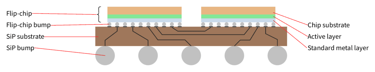
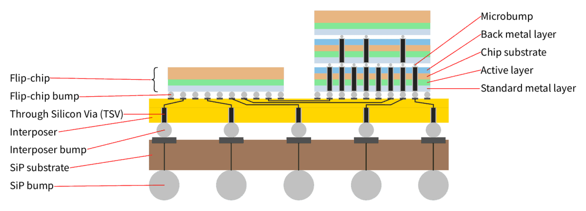
This approach is called heterogeneous integration, and the result is called a System-in-Package or SiP for short.
The easiest way is to assemble a SiP is to place two or more dies next to each other on the same substrate. The dies are interconnected with each other through wires in the substrate. The substrate also provides an external connection through tiny globes of solder—called solder bumps.
A die can be mounted face up. Then the die is connected to the interconnections and the solder bumps with wires.
More common is to mount a die face down. In this case, the die itself has microscopic solder globes—called microbumps—that come into contact with pads on the top of the substrate. These pads are, in turn, connected to the substrate’s interconnections and solder bumps.
This form of SiP is called 2D IC (two-dimensional integrated circuit) because the dies are mounted in a single plane. It is also known as multi-chip module (MCM).
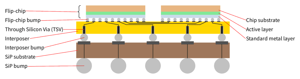
The next step up in SiP-complexity is called 2.5D IC (two and a half-dimensional integrated circuit). The name comes from the fact that dies are still side by side, but now face down on an intermediate layer of silicon—called interposer. An interposer has pads on its top and microbumps on its bottom. Horizontal electrical connections inside the silicon interconnect some pads. Some are connected to microbumps by a vertical electrical connection running through the silicon—called through silicon via or TSV for short.
So what’s the point of adding an interposer? An interposer generally reroutes connections from one configuration and pitch to another configuration and pitch. But this is not the primary reason for their use in 2.5D ICs; the same goal can be achieved with wires on the substrate in 2D ICs. It is the use of silicon that makes them worthwhile.
The fabrication techniques used for silicon allow electrical connections much finer than feasible on common substrates. Moreover, we are not constrained to connections horizontally but can also make them vertically. Thus, we can create many interconnections without a larger footprint or adding much height. In turn, this means shorter signal paths that enable higher transmission rates and reduce power losses.
In addition, silicon expands much less when heated than common substrates. More importantly, it expands like the dies mounted on top, whose microbumps must align perfectly with the pads they connect to.
The most complex SiP uses dies on top of each other. This is called 3D IC (three-dimensional integrated circuit).
In its simplest form, one die is mounted on the top of another die, with the lower die employing through-silicon vias (TSVs) to allow the upper die to connect to the lower die and to the substrate.
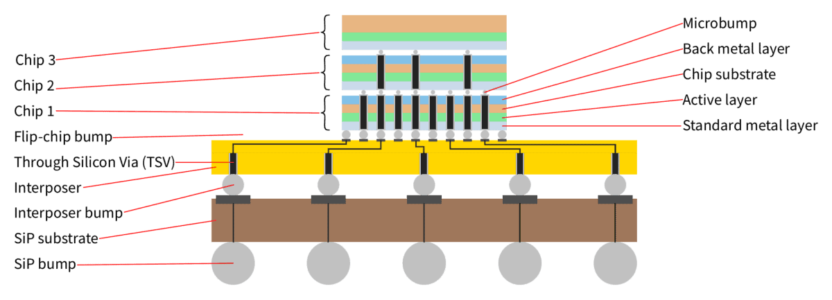
In the general case, a 3D IC consists of multiple dies stacked on top of each other using TSVs, and multiple stacks of dies interconnected through a silicon interposer. In jets, this is sometimes called 5.5D IC since it combines the techniques of 2.5D and the simplest version of 3D.
A system-in-package (SiP) is the result of heterogeneous integration. Simple dies are put together like Lego pieces to form complex systems. As we have already noted, SiP provides less footprint, increased yield, increased transmission speed, and less power loss. Taken together, this opens the door to continued rapid growth in performance per unit area despite the literal meaning of Moore’s law ceasing to apply.
However, it is not enough to open the door; we must also get through it.
Several things need to be addressed to maintain continued rapid growth in performance per unit area. In particular,
These are challenges that put boundaries for what is possible with heterogeneous integration. And we have accepted the challenge.
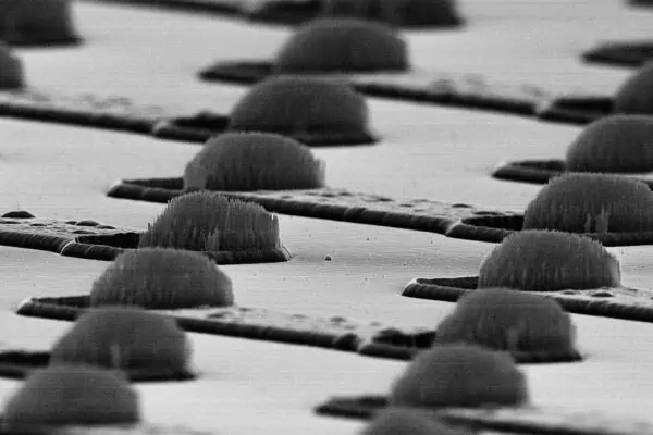
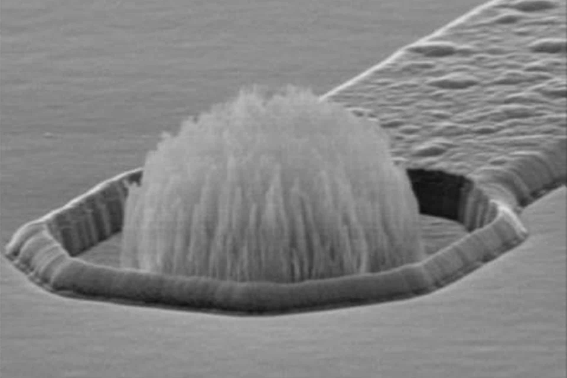
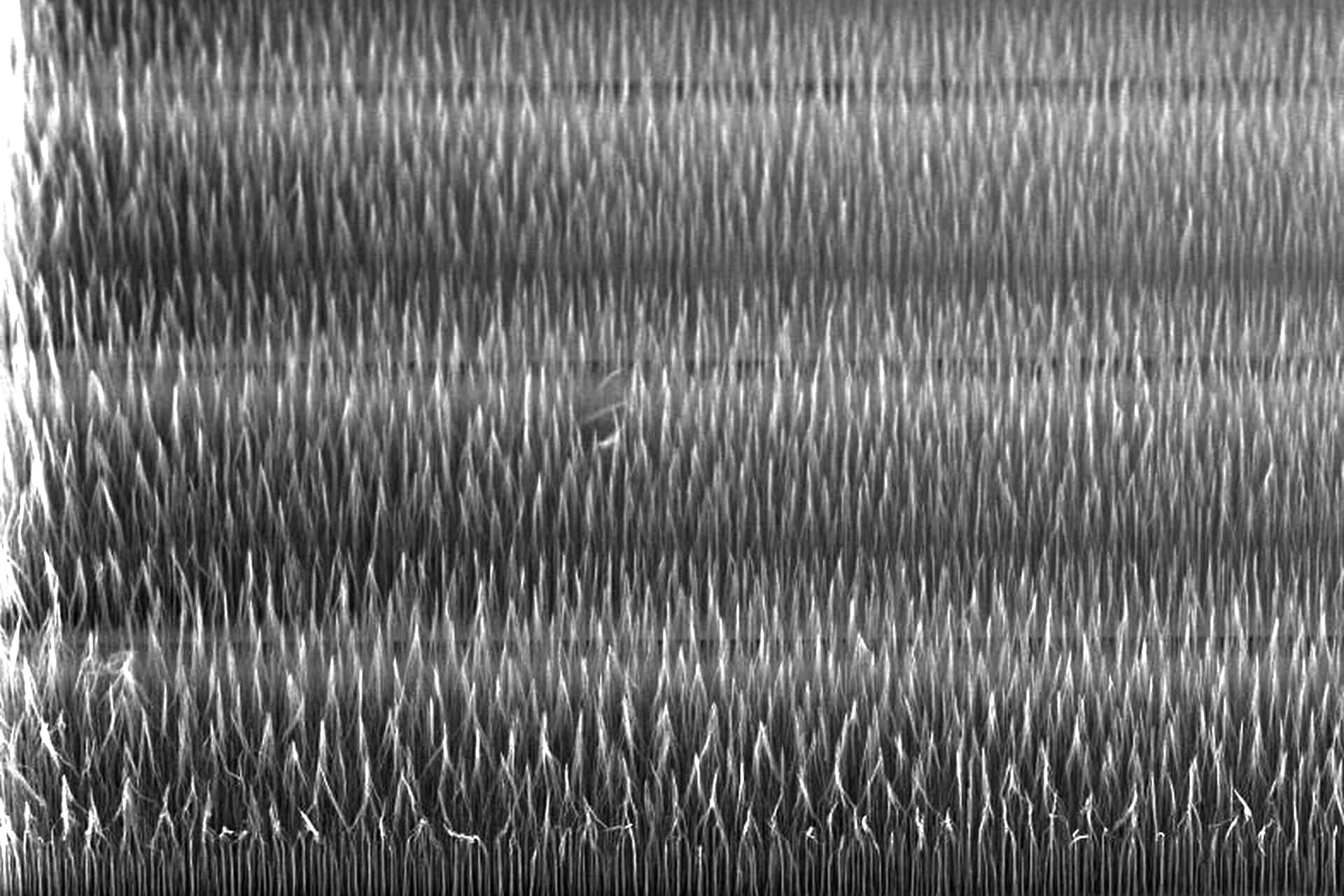
Smoltek develops technologies to fabricate nanostructures. In particular, we are focusing on carbon nanofibers (CNFs), which have many valuable properties. They are very stiff and strong. They are good conductors of heat and electricity. And the contact surface where they stand increases a thousandfold.
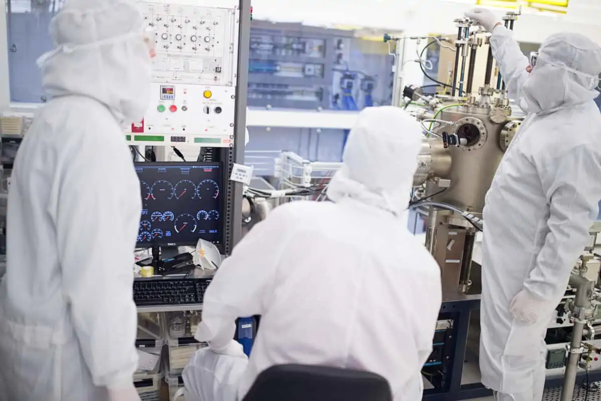
A significant part of Smoltek’s research and development has been committed to overcoming the challenges of heterogeneous integration. We have also committed ourselves to develop a fabrication technology that is process compatible with CMOS. The latter’s challenge is the relatively low temperatures used in CMOS fabrication. We are pleased to say that we have delivered on our commitments.
We have developed
These achievements form the cornerstones on which we have built Smoltek Tiger—an assembly platform concept for heterogeneous integration and advanced packagings such as 2.5D and 3D SiP.
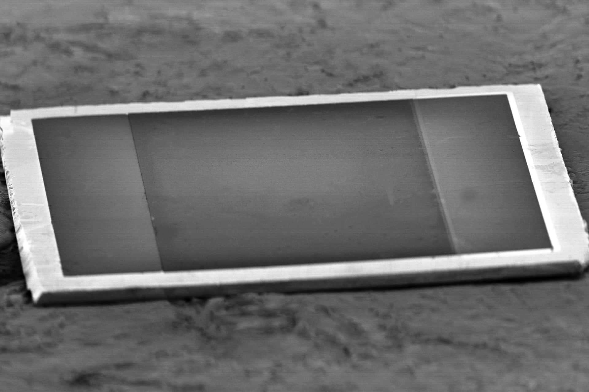
Of these achievements, we are most excited about our capacitor, which has the world’s smallest footprint (650 nF/mm2) and lowest build height (0.5–10 µm). Its internal resistance (ESR) is less than forty milliohms (40 mΩ), and its internal inductance (ESL) is below fifteen picohenry (15 pH). So, of course, we also want to make this technology available as a regular discrete component.
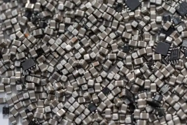
Capacitors are essential in all electronics. They store energy, attenuate transients, dissipate interference, and more. They are indispensable. Not least inside and outside integrated circuits.
We have therefore focused in particular on developing our ultra-miniaturized capacitor and making it available as a discrete component that can be
The total height, including capsule, is only 30 µm—which is less than half what is possible with other technologies.
The most amazing thing about this microscopic capacitor is its performance. One square millimeter has a capacitance of a whopping 650 nF/mm2. Its internal resistance (ESR) is less than 40 mΩ, and its internal inductance (ESL) is below 15 pH.
We describe our capacitor as a CNF-MIM capacitor since it is a metal-insulator-metal (MIM) capacitor where carbon nanofibers (CNF) are used to create a much larger surface area hence higher capacitance than the form factor suggest.
Read the dedicated page about Smoltek’s CNF-MIM capacitor for more information.

Smoltek’s business model is not to manufacture semiconductors nor capacitors but to license our fabrication technology to leading suppliers of such products.
We offer a long-term technical partnership, where we contribute our technology which we have invested money and time in developing at our peril, for the benefit of our partner, thus shortening the development time and minimizing the risks. We also offer know-how, tailor-made solutions, production of test series, and advice and assistance in implementing the manufacturing process.
Are you interested in partnering with us? Contact us today, and let’s arrange a meeting to discuss it further.
Your data will be handled in compliance with our privacy policy.

Smoltek’s focus on qualified research places it firmly in the Explorer quadrant of the R&D Evaluation Matrix, a model for assessing a company’s research and development strategy. Discover why this matters to investors and how Smoltek translates groundbreaking research into valuable business opportunities.
Smoltek’s business division for the semiconductor industry, Smoltek Semi, focuses one hundred percent on capacitors. Why? After all, a capacitor is not a semiconductor. And what is the endgame for this venture? These are questions we address in this blog post.

Håkan Persson, CEO of Smoltek, talked at the one-day conference Aktiedagen Lund organized by Aktiespararna (the Swedish Shareholders’ Association). His presentation offered some news and insights that are worth exploring further. So, let’s follow up with some questions for Håkan.
Smoltek has developed the world’s thinnest discrete capacitor. You have to stack ten of them on top of each other to reach the same height as today’s industry-standard when it comes to surface-mounted capacitors. The most amazing thing about this microscopic capacitor is its performance. One square millimeter has a capacitance of a whopping 650 nanofarads (650 nF/mm2). Read on for more details.

Smoltek holds unique world patents for technologies that make material engineering on an atomic level possible. Smoltek has solutions that allow continued miniaturization and increased performance of semiconductors, contribute to carbon-free steel production and renewable energy storage, and enable mind control of robotic prostheses. This is a story of how Smoltek came to be.

A main goal for Smoltek Semi is to develop an industrial process for mass production of discrete CNF-MIM capacitors at contract manufacturers (foundry), including a specially designed machine for large-scale production of carbon nanofibers.