Sign up for our newsletter!
Your data will be handled in compliance with our privacy policy.
Your data will be handled in compliance with our privacy policy.


Smoltek Semi has developed a process for manufacturing of engineering samples in high volumes. This process will now be tested for production of CNF-MIM engineering samples in high volumes, as the first trial-run of capacitor prototypes (without the patent protected carbon nanofibers) was successful.
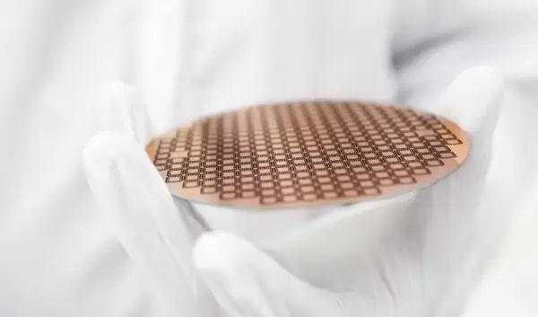
Smoltek Semi has successfully manufactured capacitor prototypes (without carbon nanofibers) on 8‑inch wafer format. The processing has been carried out in collaboration with several manufacturing partners, including research institutes, tool vendors as well as high-volume foundries. Most of the processing has been made on standard high-volume production tools used for component production in the semiconductor industry.
The capacitor prototypes have the purpose of developing and validating the stability, repeatability, and overall quality of the fabrication processes necessary for 8‑inch wafer format production – not to demonstrate high electrical performance of our CNF-MIM capacitors.
Louise Duker, Chief Product Officer at Smoltek Semi.
Based on the successful results achieved, Smoltek Semi has decided to utilize the developed 8‑inch fabrication process to produce the first lot of CNF-MIM engineering samples, incorporating Smoltek’s proprietary and patent-protected carbon nanofibers.
The CNF-MIM engineering samples, that are now being manufactured in this 8‑inch process are expected by the end of the fourth quarter this year. The electrical performance, reliability and process stability that Smoltek Semi aims to demonstrate with these CNF-MIM engineering samples will provide information needed to take the next step towards a commercial high-performing capacitor product together with our partner YAGEO.
Development of a more industrial production process
This process development is important for primarily two reasons. The first being the significant increase in the number of capacitors we can produce for development purposes, approximately 27 000 capacitors on one single 8‑inch wafer.
The sheer number makes it possible to conduct more data-driven development, and hence accelerate the development pace towards a commercial product.
Karl Lundahl, COO and Head of R&D at Smoltek Semi.
The second reason why the 8‑inch form factor is important is that the format is compatible with high-volume production.
We are quite confident that the 8‑inch wafer format that we now have migrated to in our development will enable us to more effectively expedite the tech-transfer of the fabrication processes to a future high-volume production setting.
Karl Lundahl, concludes.
Your data will be handled in compliance with our privacy policy.

Smoltek holds unique world patents for technologies that make material engineering on an atomic level possible. Smoltek has solutions that allow continued miniaturization and increased performance of semiconductors, contribute to carbon-free steel production and renewable energy storage, and enable mind control of robotic prostheses. This is a story of how Smoltek came to be.

Smoltek has been granted three new patents since the start of the year. The patents are related to three different families: Interconnects, Assembly platform and Compact energy storage interposer. This makes our patent portfolio to now comprise 68 granted patents in total.

Smoltek has yet another patent granted. This time in India. The patent is related to the growth process of nanostructures and it makes the Catalyst diffusion patent family complete.
The constantly expanding Smoltek IP-portfolio is divided into several different patent families. One of them is named Helplayer, a method to protect the underlaying materials when growing nanostructures on a given surface. To this family we can add another patent number recently granted.

Smoltek’s proprietary platform keeps growing as we have been awarded another approved patent. This new US patent covers energy storage devices and the usage of the same. Our patent portfolio now comprises 60 granted patents.
Smoltek is awarded a new patent. This Korean patent is the second of a patent family in the direction of CNF-MIM based compact energy storage interposers. This means that our patent portfolio now comprises 56 granted patents.