Sign up for our newsletter!
Your data will be handled in compliance with our privacy policy.
Your data will be handled in compliance with our privacy policy.

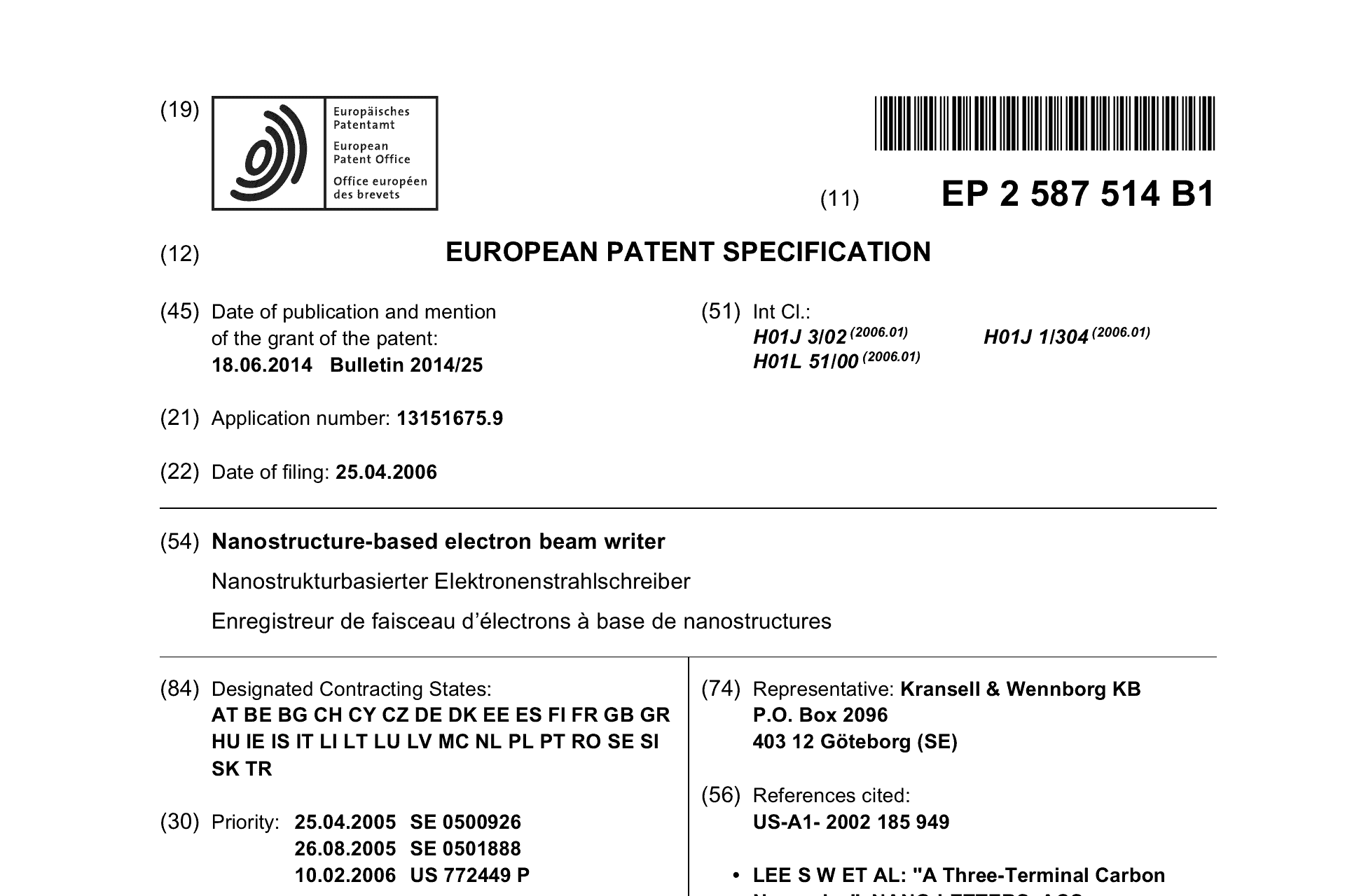
The Nanostructure E-beam writer family is covering a method for the manufacture of an integrated circuit comprising nanostructures.
S Kabir • April 25, 2006
The invention: A nanostructure-based electron beam writer. The innovation is an electron beam writer that enables the creation of carbon nanostructures with great precision and desired properties. For example, it is possible to create a single carbon nanofiber (CNF) of a specific length, diameter and slope at a specific location.
| Patent Office | Patent |
|---|---|
| China | CN101313092 |
| Europe | EP1945840 |
| Japan | JP5519936 |
| South Korea | KR101365341 |
| South Korea | KR101386268 |
Your data will be handled in compliance with our privacy policy.