Sign up for our newsletter!
Your data will be handled in compliance with our privacy policy.
Your data will be handled in compliance with our privacy policy.

Smoltek uses a global patent strategy to protect our technology platform in all important markets. This includes core patents as well as patent protection at application level.
The strategic and continuous development of our patent portfolio is driven by the need for disruptive materials and technical solutions addressing critical challenges in advanced semiconductor packaging, energy storage, and hydrogen production. In this strategy, the company has prioritized application-driven filings that directly underpin commercial opportunities. This approach ensures a strong, relevant, and cost-effective IP portfolio to protect Smoltek’s innovations.
Patents
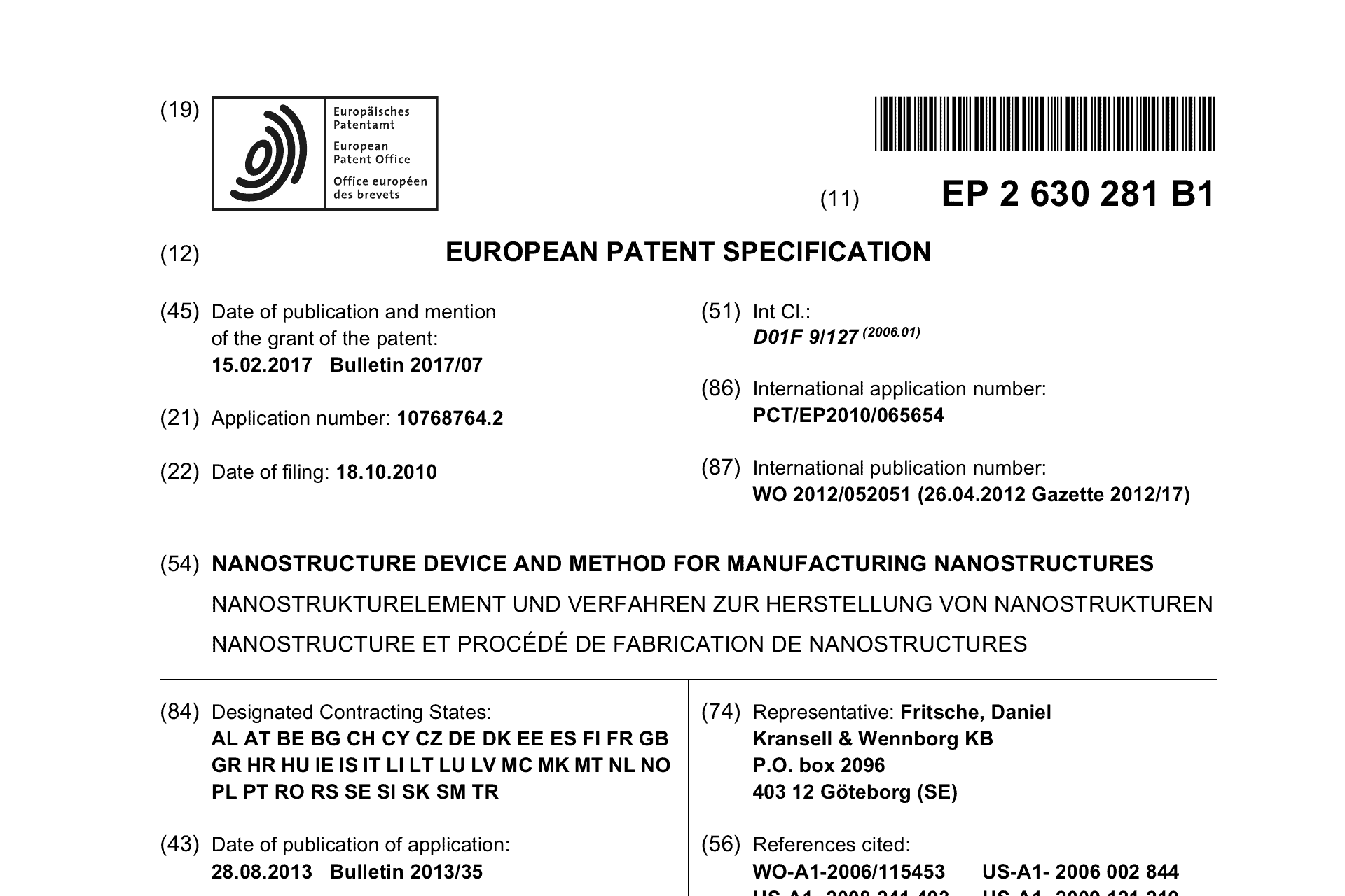
October 18, 2010
The Catalyst Diffusion family is covering a method for manufacturing a plurality of nanostructures on a substrate.
Patents
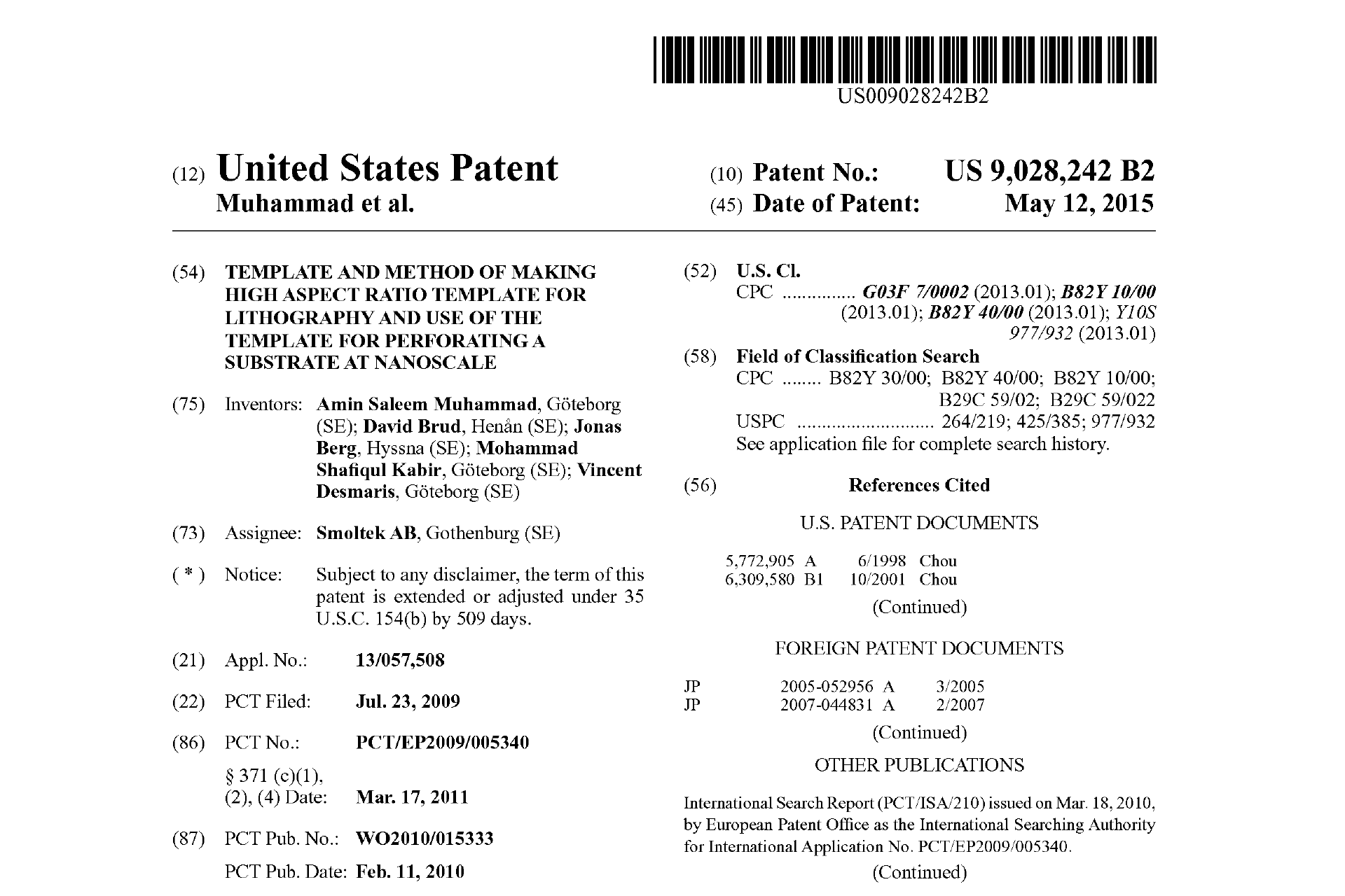
July 23, 2009
The Nano Imprint Lithography family is covering a method of making high aspect ratio template, stamp, and imprinting at nanoscale using nanostructures.
Patents
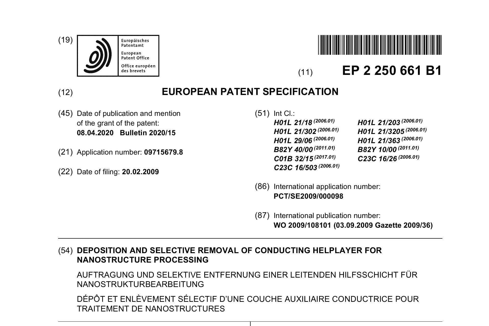
February 20, 2009
The Helplayer family is covering a method to protect the underlaying substrate or materials from being damaged during the nanostructure growth process.
Patents
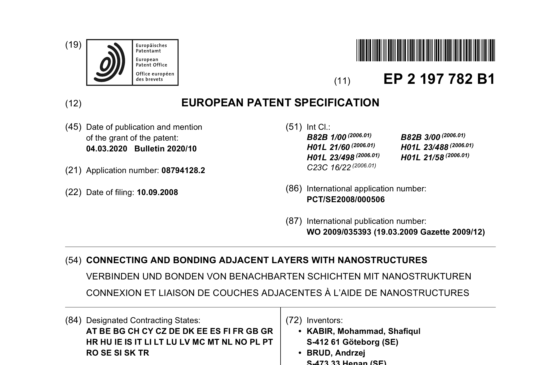
September 10, 2008
The Bumping family is an apparatus connecting and bonding adjacent layers with nanostructures.
Patents
August 28, 2006
The Interconnects B family is covering how nanostructures can be used as interconnects and/or for dissipating heat from electronic devices.
Patents
August 28, 2006
The Nanostructure IC family is covering a method for the manufacture of an integrated circuit comprising nanostructures.
Patents
April 25, 2006
The Interconnects A family is covering a method regarding controlled growth of a nanostructure on a substrate, and electron emission devices based on the same.
Patents
April 25, 2006
The Nanostructure E-beam writer family is covering a method for the manufacture of an integrated circuit comprising nanostructures.